Micron-Level Defect Detection in PCB and Electronics components Using Machine Vision AI
Published on: Sep 11, 2025

Written by: Content team, Intelgic
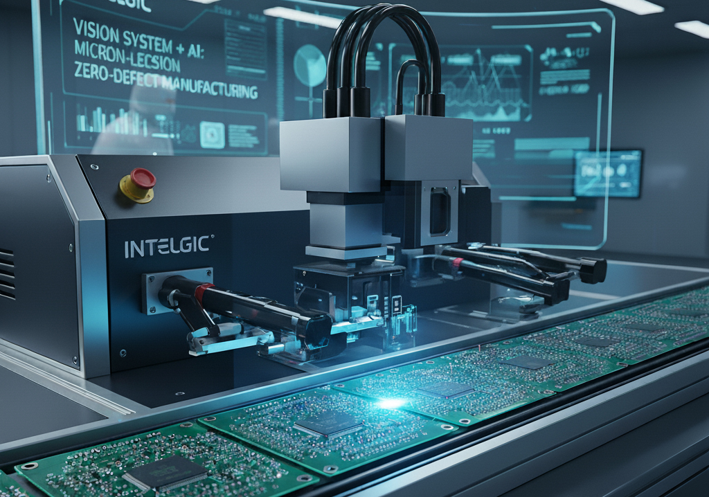
Replace Microscope and Stereoscope with Intelgic’s Powerful Vision System and AI
The miniaturization of electronics has pushed printed circuit board (PCB) assembly to extreme precision. Surface Mount Devices (SMDs) such as 0201 (0.6 × 0.3 mm) and 0402 (1.0 × 0.5 mm) packages are now common in smartphones, medical devices, automotive ECUs, and aerospace electronics. While these tiny components enable compact, high-performance designs, they also introduce micron-level defect risks in placement, soldering, and assembly.
Manual inspection or traditional AOI systems struggle to detect these microscopic anomalies reliably. AI-powered machine vision brings the capability to detect sub-10 micron defects with consistency, scalability, and speed—ensuring zero-defect manufacturing in advanced PCB production.
Challenges in Micron-Level Defect Detection on 0201/0402 SMDs
- Tiny Dimensions
- 0201 = ~0.6 × 0.3 mm
- 0402 = ~1.0 × 0.5 mm
Even a 5–10 µm defect (e.g., solder void, misalignment) can compromise functionality.
- 0201 = ~0.6 × 0.3 mm
- High Component Density
Modern PCBs pack hundreds or thousands of these components in small areas, leaving little room for error in imaging.
- Defect Variety
- Misalignment, rotation, or tombstoning
- Insufficient/excess solder paste
- Micro-cracks in solder joints
- Bridging between adjacent pads
- Foreign particles/contamination
- Misalignment, rotation, or tombstoning
- Optical Challenges
- Shiny solder joints produce glare and reflections.
- Variations in PCB color and solder mask affect contrast.
- Shiny solder joints produce glare and reflections.
Depth-of-field limits in optics when inspecting densely populated boards.
Traditional Image Processing vs. AI in PCB AOI
Traditional AOI (Rule-Based)
- Relies on golden board comparison, thresholding, and template matching.
- Effective for larger components but fails to consistently detect micron-level defects on 0201/0402 packages.
- Generates high false positives due to lighting variations and board warpage.
AI-Driven AOI (Deep Learning & Anomaly Detection)
- Learns defect patterns directly from high-resolution image datasets.
- Can identify both known and unknown defect types.
- More tolerant of natural variations in solder joint appearance, reducing false rejects.
Capable of pixel-level segmentation, enabling sub-micron accuracy in defect localization.
Technologies Enabling Micron-Level PCB Defect Detection
1. High-Resolution Machine Vision Cameras
- 5–25 megapixel industrial cameras with small pixel sizes (2–3 µm).
- Line-scan or area-scan cameras depending on inspection speed and coverage.
- Microscope-level optics integrated for magnification of 0201/0402 features.
2. Specialized Optics and Lenses
- Telecentric lenses for distortion-free imaging at micron scale.
- Adjustable focus/zoom for different PCB layers.
- Multi-focus imaging to overcome depth-of-field limitations.
3. Advanced Lighting Geometry
- Coaxial lighting for uniform illumination of solder pads.
- Low-angle darkfield lighting to highlight surface cracks and bridges.
- Multi-wavelength LEDs (UV, visible, IR) to enhance material contrast.
4. AI-Powered Defect Detection Software
Intelgic’s Live Vision AI system integrates:
- Deep learning classification of defects (e.g., missing vs. misaligned SMDs).
- Anomaly detection models trained on normal solder joints to flag unseen defects.
- Pixel-level segmentation for crack detection down to <10 µm resolution.
- Automated pass/fail decisions with defect type categorization.
5. Robotic Motion & Multi-Angle Imaging
- X-Y gantry or robotic stages for high-density boards.
Multi-angle imaging to eliminate hidden defects caused by occlusion or reflection.
Benefits of AI-Based Micron-Level PCB Inspection
- Improved Yield: Captures defects invisible to traditional AOI.
- Zero-Defect Manufacturing: Ensures reliability in mission-critical electronics.
- Reduced False Alarms: AI distinguishes real defects from harmless variations.
- Scalability: Easily adapts to new PCB designs or SMD packages.
Traceability: Generates digital inspection records and quality certificates for audits and warranty.
Real-World Applications
- Smartphones & Consumer Electronics – Detecting solder joint voids on ultra-miniature SMDs.
- Automotive Electronics – Ensuring robust assembly of ECUs, ADAS boards, and infotainment systems.
- Medical Devices – High-reliability inspection for implants, diagnostic equipment, and wearables.
Aerospace & Defense – Micron-level defect detection ensures long-term reliability in avionics systems.
Intelgic’s Solution
Intelgic delivers turnkey AOI solutions for PCB assembly lines, integrating:
- Industrial cameras and telecentric optics for micron-scale imaging.
- Specialized lighting modules for reflective solder inspection.
- AI-driven Live Vision software for detection, classification, and reporting.
- Integration with MES/ERP systems and Digital Quality Certificates (DQC) for full traceability.
Conclusion
Micron-level defects on tiny SMD components like 0201 and 0402 demand inspection precision beyond human capability and traditional rule-based AOI. AI-powered machine vision systems provide the required accuracy, adaptability, and reliability to detect micro-defects and ensure high-quality PCB assembly.
By combining high-resolution optics, advanced lighting geometry, robotic imaging systems, and AI anomaly detection, manufacturers can achieve zero-defect electronics production and meet the stringent demands of automotive, aerospace, and medical sectors.