0201/0402 SMD Inspection — Automated Microscopic Quality Control with AI

  • Gentex logo
  • RxSight logo
  • magna logo
  • clariant logo
  • 1800Accountant logo
  • Eptisa logo
  • Aptive logo
  • Save A Lot logo
  • TCS Transportation logo
  • Solid logo
  • Dareesoft logo
  • Petromin logo
  • CostaRicaABC logo
  • Fenice Energy logo
  • Linde logo
  • Cummins logo
  • Sammons Industrial logo
  • Mobile Maintenance logo
  • Link-X logo

Automate what you currently check under a microscope.

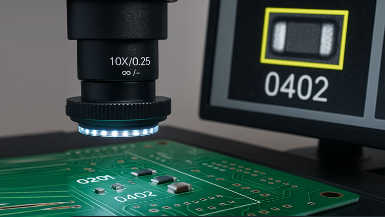
Intelgic replaces manual microscopic inspection of ultra-miniature SMDs (0201: ~0.6×0.3 mm, 0402: ~1.0×0.5 mm) with a high-resolution imaging system and AI-powered defect detection that reliably catches sub-10 µm issues—at production speed.

Micron-level Accuracy

Consistent Pass/Fail

Full Traceability (DQC)

Manual microscope inspection

Manual Inspection is Slow and Inconsistent

Manual microscope inspection is slow, subjective, and hard to scale. Tiny variations in lighting, fatigue, or interpretation lead to misses and false rejects—especially on dense PCBs packed with 0201/0402 parts. Intelgic’s automated AOI station delivers repeatable, objective results, integrates with your line, and generates digital records for audits and warranties.

What Intelgic Automates (Typical Defects)

Placement

Offset/shift, rotation, skew, tombstoning, tilt

Solder

Insufficient/excess solder, bridging, opens, voids, wetting issues

Joint integrity

Micro-cracks, cold joints, fillet shape anomalies

Component

Missing/polarity wrong, counterfeit/marking mismatch (OCR), package damage

Foreign matter

Fibers, dust, flux residues, solder balls

PCB features

Pad damage, solder mask delamination, mask encroachment

System Overview

Imaging Hardware

  • Industrial cameras: 20–65 MP with 2–3 µm pixels for micron-scale resolution
  • Telecentric lenses: distortion-free metrology on tiny leads and fillets
  • Lighting geometry (software-controlled): coaxial brightfield, low-angle darkfield, polarized ring, multi-wavelength (UV/Vis/IR) to reveal glare-prone solder details
  • Precision motion: X-Y stage or gantry; optional Z-axis autofocus for uneven boards; fiducial-based alignment

Live Vision AI (Intelgic)

  • Deep learning + anomaly detection: learns “good” joints and flags outliers—ideal when labeled defect data is scarce
  • Pixel-level segmentation: measures defect area/length; supports thresholds in µm or pixels
  • Multi-class classification: defect type, severity grading, component presence/polarity
  • Adaptive recipes: switch models/parameters per product or panel step; A/B changeover in minutes
  • Analytics & DQC: per-board/per-joint records, trends, heat-maps, Digital Quality Certificates for every PASS unit

Throughput & Integration

  • Inline or offline: integrates after SPI/placement/reflow, or as a bench-top cell
  • Comms: MES/ERP/PLC via OPC-UA, REST, SQL; barcode/QR linking
  • User roles: operator, QA engineer, admin; audit trail & versioned recipes

How It Works (Workflow)

1

Load & Align

Panel enters station; fiducials auto-align the field of view.

2

Programmed Imaging

The system executes a scan path; lighting modes switch to expose different defect signatures.

3

AI Inspection

Models classify/segment defects, compute metrics, and apply acceptance criteria.

4

Decision & Actions

PASS/FAIL per component, with optional mark/reject/stop-line outputs.

5

Record & Report

Results stored with timestamps, images, measurements, lot/serial; DQC issued for PASS boards.

Performance at a Glance

Defect sensitivity

< 10 µm (application-dependent; optics & lighting optimized per board)

Placement accuracy check

±5–10 µm typical with telecentric optics

False rejects

Reduced vs. rules-based AOI through learned normal-appearance modeling

Changeover

New product recipe loading in minutes; model fine-tuning supported

Why Telecentric + AI Matters for 0201/0402

  • Telecentric optics remove perspective error → trustworthy micrometer measurements on pads, leads, and fillets.
  • AI anomaly detection doesn’t need every defect label → rapid deployment even when true defects are rare.
  • Lighting orchestration reveals solder topography and micro-cracks that single-mode illumination can hide.

Acceptance Criteria (Examples)

(Defined with your QA team; below are common defaults.)
  • 0201/0402 placement offset ≤ 25 % pad width; rotation ≤ 5°
  • Solder bridge gap ≥ 20 µm; solder ball diameter ≤ 50 µm and count per zone thresholds
  • Fillet coverage ≥ pad rule; void fraction ≤ x % (per IPC class)
  • Crack length

Data, Traceability & DQC

  • Per-component logs: images before/after decisions, defect masks, metrics in µm
  • Lot/serial binding: scan board ID; auto-associate to work order and recipe version
  • Dashboards: FP/FN trend, top defect Pareto, station OEE, heat-maps across the panel
  • DQC: digitally signed certificate for every PASS board; cloud or on-prem storage

Comparison: Manual Microscope vs Intelgic AOI

Aspect Manual Microscope Intelgic AOI
Consistency Operator-dependent AI criteria, repeatable
Speed Slow; non-scalable Inline, panel-level fast scans
Sensitivity Limited by fatigue Sub-10 µm with high-mag optics
Records Sparse notes/photos Full image & metric archive + DQC
Changeover Retrain humans Load recipe; optional quick re-train
Cost of Quality High rework/escape risk Lower false rejects & escapes

Frequently Asked Questions

Yes. Most customers migrate to automated AOI for primary decisions and keep minimal spot-checks for audit.

No. We bootstrap with good-only anomaly models and incrementally add labeled defect data to refine classes.

We mitigate with coaxial + polarized + darkfield lighting and train models on varied exposures for robustness.

Yes. We design the scan path, FOV tiling, and inference pipeline to your cycle time; parallel cameras are available for high-throughput lines.

Telecentric optics, stage calibration, and per-recipe scale validation (grid targets) ensure µm-accurate metrology.

Say hello to Intelgic

contact intelgic
Book a call

©2025 Intelgic Inc. All Rights Reserved.