Automated PCB Inspection Using Machine Vision and AI
Published on: Jul 16, 2025

Written by: Content team, Intelgic
Introduction
Printed Circuit Boards (PCBs) are the backbone of all modern electronic devices, from consumer gadgets to automotive control systems and industrial automation. As PCBs grow increasingly complex—with high component density, miniaturized chips, and multi-layer structures—manual inspection becomes infeasible. Manufacturers now demand automated, accurate, and high-speed inspection systems to ensure quality, prevent failures, and reduce rework costs.
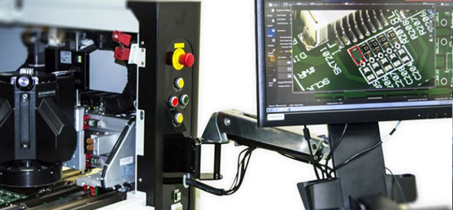
Intelgic provides a comprehensive AI-driven PCB inspection solution, combining high-resolution machine vision, robotic motion systems, and powerful AI algorithms to inspect PCBs for defects, component accuracy, and placement validation.

Challenges in PCB Board Inspection
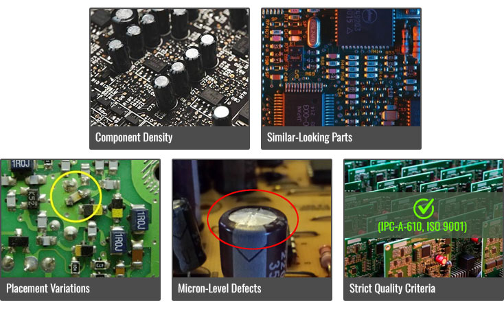
Inspecting PCBs is a technically demanding task due to the following challenges:
Component Density: Modern PCBs may contain hundreds of micro-components in tight spaces.
Similar-Looking Parts: Differentiating between capacitors, resistors, and ICs of similar size and color requires high-resolution imaging and intelligent classification.
Placement Variations: Minor rotational or positional shifts can cause critical failures.
Micron-Level Defects: Cracks in solder joints, lifted pins, or scratches in substrate need inspection at sub-millimeter or even micron resolution.
Strict Quality Criteria: Every product must pass industry-specific acceptance standards (IPC-A-610, ISO 9001, etc.).

System Overview: Intelgic’s Vision-Based PCB Inspection Platform
Intelgic’s solution addresses all these challenges using a multi-layered system architecture:
1. High-Resolution Area Scan Camera
Captures detailed 2D images of static or semi-static PCB assemblies.
Supports pixel-level image clarity required to identify small passive components, IC labels, pin locations, and solder points.
2. Precision Industrial Lenses
Telecentric lenses eliminate distortion and enable accurate dimensional measurements across uneven PCB surfaces.
Macro lenses are used for high-detail close-up inspections.
3. Advanced Illumination System
Coaxial lighting for inspecting reflective solder joints.
Dark field illumination to highlight fine surface scratches and cracks.
Multi-angle LED arrays to reduce shadows and enhance depth visualization.
4. Robotic Motion System (X-Y-Z Movement)
Intelgic integrates automated motion platforms to move the camera or PCB under inspection across the X, Y, and Z axes.
This motion ensures every region of interest is captured from the ideal focal distance and angle.
Enables multi-frame imaging, essential for inspecting larger boards or parts at varying depths (e.g., connectors vs. surface-mount chips).

AI-Based Image Processing and Defect Detection
Once images are acquired, Intelgic’s Live Vision AI software performs advanced image processing and classification:
Defect Detection
Detects open circuits, solder bridges, cracks, lifted pins, missing solder, burn marks, and surface contamination.
Flags scratches or delamination on PCB substrate.
Component Identification and Verification
Reads text, codes, and identifiers printed on chips and passive components.
Matches detected parts to the expected part list (Bill of Materials) and verifies their position, orientation, and alignment.
Component Counting
Counts and classifies components like resistors, capacitors, transistors, and ICs across the entire board.
Confirms if all required parts are present based on predefined templates.
Pass/Fail Classification
After all features and measurements are processed, the system applies user-defined acceptance criteria to decide whether a board passes or fails.
Optionally integrates with MES or quality control systems for traceability and logging.

Workflow Summary
1. PCB is positioned under camera (either fixed or moving via motorized stage).
2. Lighting and camera parameters are optimized for current board type.
3. Multiple images are captured (depending on board size and complexity).
4. Images are processed using Intelgic’s AI algorithms.
5. Detected components and defects are compared against the design spec.
6. A real-time PASS/FAIL decision is displayed.
7. Results are logged in the system with part ID, defect type, and image proof.
Key Features of Intelgic’s PCB Inspection System
AI-Powered Defect Detection: Learns from labeled data and adapts to new board types and component layouts.
Recipe-Based Inspection: Easily switch inspection parameters for different PCB models using pre-configured templates.
Traceability and Reporting: All inspection data, including defect locations and images, are stored for future analysis, quality audits, and warranty support.
Scalable Architecture: Supports small-batch labs to high-speed SMT production lines.
Benefits
Accuracy Sub-millimeter defect detection and component verification.
Speed Supports inline inspection with minimal impact on throughput.
Repeatability Eliminates human error and subjectivity in inspection.
Cost Reduction Prevents downstream failures, reduces rework, and improves first-pass yield.
Flexibility Adaptable to various PCB sizes, layouts, and production environments.
Conclusion
As PCB complexity continues to rise, Intelgic’s AI-powered machine vision system offers an intelligent, scalable, and highly accurate solution for PCB inspection automation. With a combination of area scan imaging, robotic motion control, custom illumination, and deep-learning algorithms, Intelgic ensures that your production line delivers only the highest quality boards—efficiently and cost-effectively.
Whether you're building medical electronics, automotive controllers, or consumer electronics, Intelgic’s PCB inspection solution delivers the precision and reliability required for today’s zero-defect manufacturing goals.

