Dual-Surface PCB Inspection for Missing Components Advanced Machine Vision AOI
Published on: May 15, 2025

Written by: Content team, Intelgic
Dual-Surface PCB Inspection for Missing Components Using Machine Vision AOI
In modern electronics manufacturing, ensuring the integrity of printed circuit boards (PCBs) is critical to product reliability and performance. Among various defects that can affect PCB quality, missing components such as resistors, capacitors, and inductors, as well as soldering faults, are among the most common and challenging to detect—especially on double-sided boards. Traditional inspection methods often fall short in handling these challenges efficiently. However, with the advancement of Machine Vision Automated Optical Inspection (AOI) systems, it is now possible to perform precise, high-speed, and comprehensive inspections on both surfaces of a PCB, enabling manufacturers to achieve higher yield and better quality control.
Understanding the Challenges in PCB Inspection
Inspecting PCBs for missing components and soldering issues presents a unique set of challenges, particularly as board complexity increases. Each surface of the board—top and bottom—brings its own obstacles, and various environmental and material factors complicate the inspection process. Below are some of the most significant challenges faced:
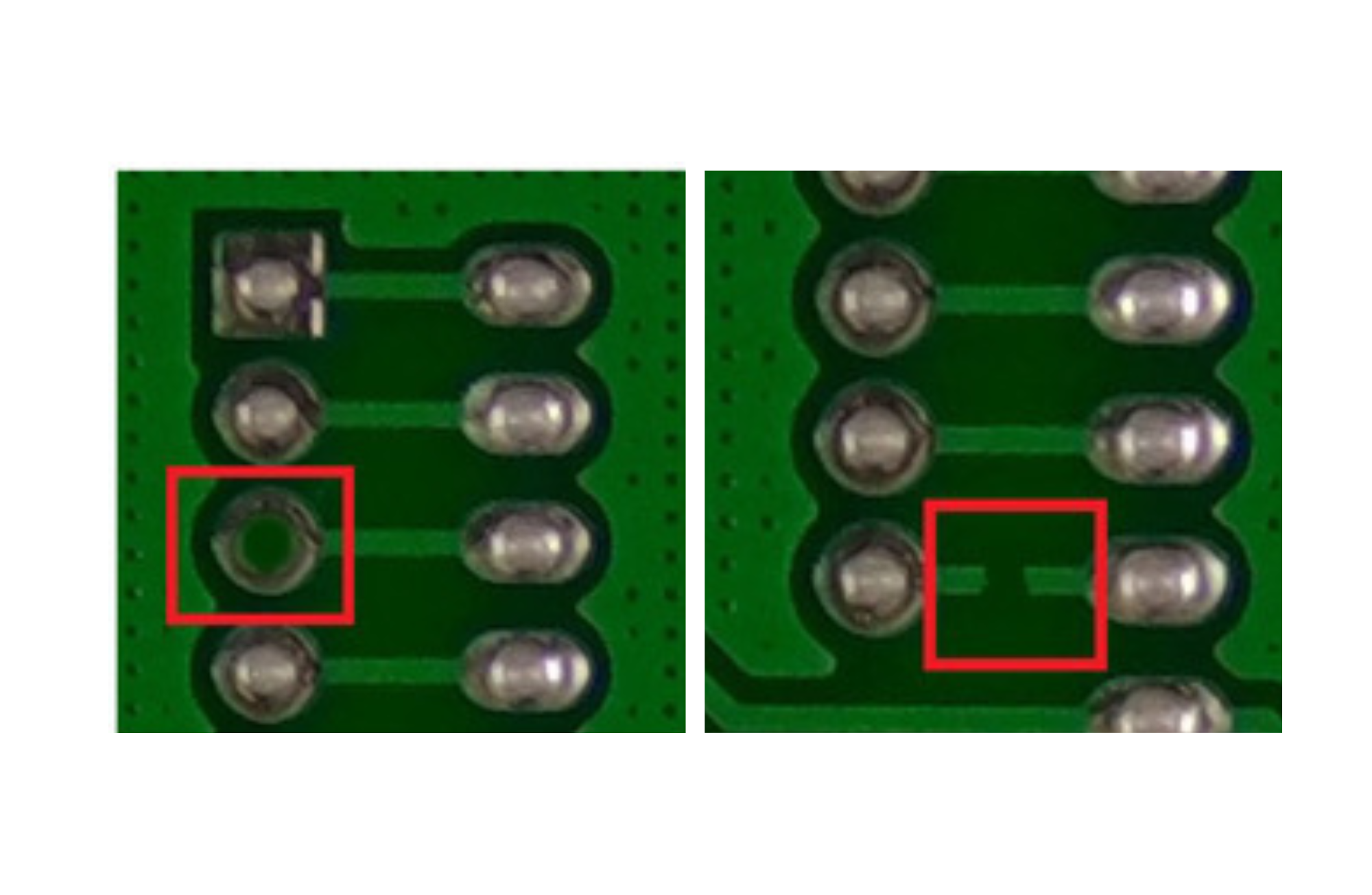
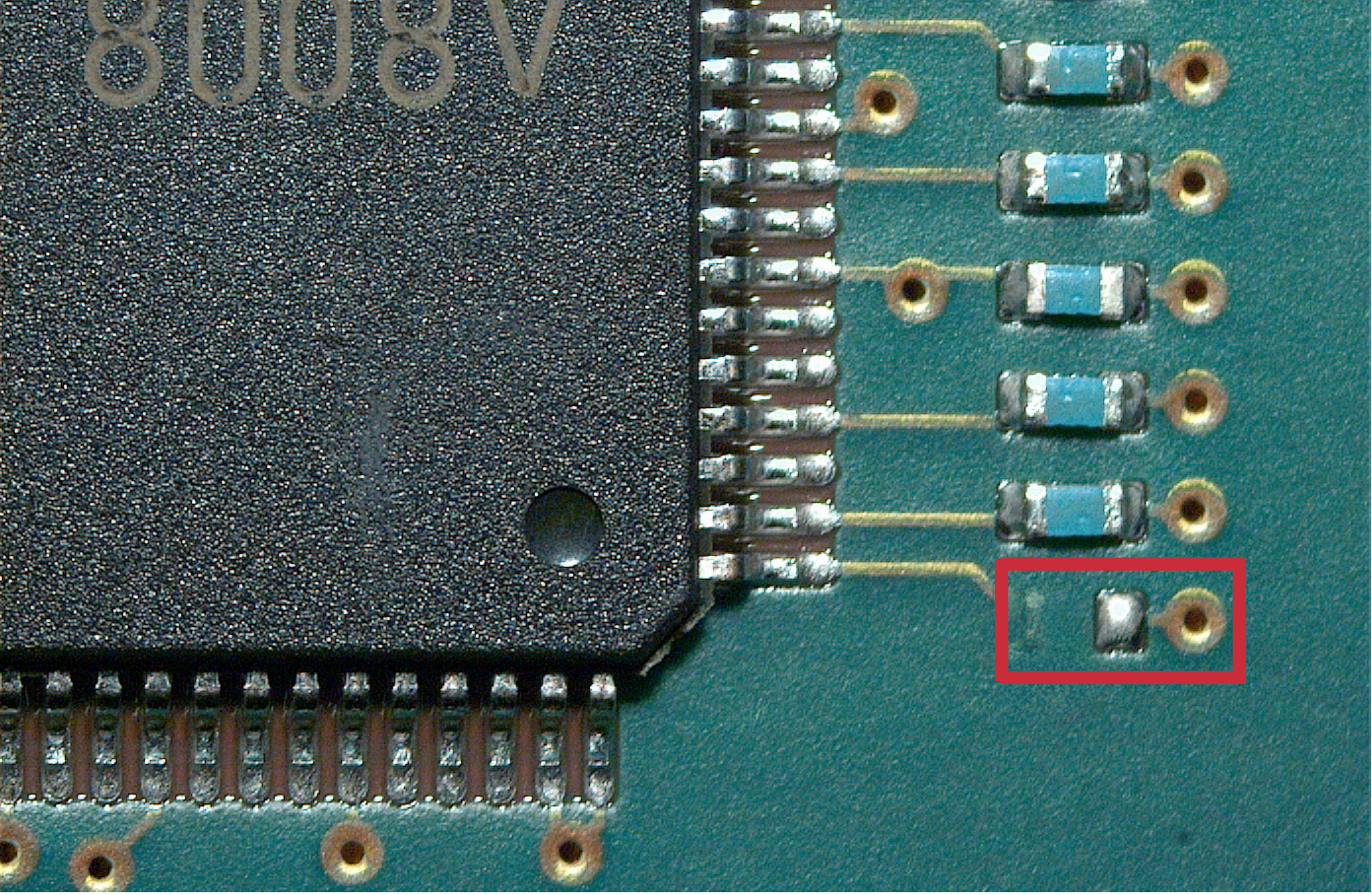
1. Missing and Misplaced Passive Components
Tiny components such as resistors, capacitors, and inductors are easily overlooked due to their size and uniform appearance. These components are often packed closely together, and even a single missing part can compromise the functionality of the entire circuit.
2. Soldering Defects on the Bottom Surface
In double-sided PCBs, the bottom (or solder) side often contains surface-mounted devices (SMDs) and through-hole components whose solder joints are difficult to inspect. Common soldering issues include cold solder joints, insufficient solder, solder bridges, and voids—many of which are nearly impossible to detect with the naked eye.
3. Component Orientation and Polarity Errors
Some components, such as diodes, electrolytic capacitors, and integrated circuits, are polarity-sensitive. Incorrect orientation can lead to circuit failure and is a frequent error in fast-paced assembly lines.
4. Human Error and Fatigue in Manual Inspection
Manual inspection relies heavily on the operator’s skill and focus, which can degrade with time. Fatigue can lead to missed defects or inconsistent judgment, especially over long production shifts or with high-volume runs.
5. Reflective Surfaces
Many components and solder joints have reflective surfaces that can interfere with visual and optical inspection. These reflections can create glare, false edges, or ghost images that confuse traditional imaging systems, leading to inaccurate detection or false positives.
Machine Vision AOI: A Technological Solution to Complex Inspection Demands
Machine Vision AOI has emerged as a transformative solution to these challenges, offering precision, repeatability, and adaptability. When configured with dual area scan cameras, advanced illumination, and AI software, these systems can inspect both surfaces of a PCB efficiently and reliably.
Dual-Surface Inspection with Area Scan Cameras
In stationary PCB inspection systems, area scan cameras play a pivotal role in delivering high-resolution, full-frame images of the board’s surface. Unlike line scan cameras, which capture images one line at a time and require relative motion between the camera and the object, area scan cameras capture the entire field of view in a single exposure. This makes them particularly well-suited for stationary AOI (Automated Optical Inspection) setups, where the PCB remains fixed during inspection.
Using two high-resolution area scan cameras, the AOI system inspects the PCB from both top and bottom simultaneously or in sequence. These cameras are positioned strategically:
- Top Camera: Captures detailed images of the component placement on the top layer.
- Bottom Camera: Focuses on solder joints, leads, and component positions on the reverse side.
This dual-camera setup eliminates the need to manually flip boards and enables seamless inspection in one pass.
Intelligent Illumination for Reflective Materials
Inspecting reflective materials such as metallic components, solder joints, and polished PCB surfaces poses significant challenges due to glare, specular reflections, and uneven lighting. To overcome these obstacles, intelligent illumination systems are employed, utilizing a combination of advanced lighting techniques tailored to enhance image clarity and inspection accuracy.
These techniques include:
- Multi-Angle Lighting: Projects light from various angles to reveal surface details and minimize shadowing.
- Diffuse Illumination: Softens and spreads light uniformly across the surface to reduce harsh reflections, especially useful for glossy or uneven textures.
- Coaxial Lighting: Directs light along the same axis as the camera lens, ideal for detecting fine surface defects and inspecting flat, reflective components.
- Structured Illumination: Uses patterned or directional light to enhance depth perception and highlight subtle surface variations.
By intelligently controlling the type, angle, and intensity of illumination, the system can significantly reduce false positives caused by lighting artifacts. This allows the AOI system to accurately distinguish between genuine defects and benign reflections, ensuring reliable inspection of even the most challenging reflective surfaces.
AI-Powered Software for Advanced Analysis
Trained on thousands of labeled PCB images, the AI-powered software leverages deep learning to conduct advanced comparison and defect recognition with exceptional accuracy. It effectively detects missing or misplaced components, incorrect orientation, and a wide range of soldering defects—such as insufficient solder, bridging, and cold joints—surpassing the capabilities of traditional rule-based inspection systems.
Upon identifying a defect, the AI system automatically generates real-time alerts through the AOI interface, designed to promptly notify operators and streamline defect resolution. These alerts include:
- Visual Annotations: Defects are clearly highlighted on inspection images using color-coded bounding boxes or overlays for immediate identification.
- Defect Labels: Each detected issue is classified (e.g., “Component Missing,” “Solder Bridge”) to provide clear and actionable insights.
- Severity Indicators: Alerts are prioritized by defect severity, enabling operators to focus on the most critical issues first.
- Inspection Logs: All anomalies are systematically recorded to support traceability, quality control reporting, and ongoing process improvement.
The AI software continuously refines its detection capabilities by incorporating operator feedback and adapting to new PCB designs and component types. This self-learning functionality ensures the system remains highly effective in evolving manufacturing environments, maintaining optimal inspection performance across diverse production scenarios.
Step-by-Step Description of the AOI Inspection Process
- PCB Loading
The process begins with an automated PCB loader, which gently feeds each board into the inspection station to ensure precise positioning.
- Top Surface Imaging
The first area scan camera captures high-resolution images of the PCB’s top side, focusing on component placement, polarity, and alignment.
- Bottom Surface Imaging
The second area scan camera images the bottom of the PCB, inspecting for solder joint quality, missing bottom-side components, and through-hole integrity.
- Image Processing and AI Analysis
The captured images are processed in real time by AI-enabled software, which compares them to known good references or uses trained models to identify anomalies such as missing components, misplacements, and soldering faults.
- Defect Classification and Reporting
Detected defects are clearly marked and classified on-screen for operator review. Each inspection result is logged and can be exported for quality reports and traceability.
- Unloading and Sorting
After inspection, the board is automatically passed to the PCB unloader, where defective boards can be routed for rework while good boards proceed to the next stage in production.
Advantages of Using Machine Vision AOI for PCB Inspection
- Comprehensive Inspection Coverage: Ensures complete visibility of both PCB surfaces without manual flipping.
- Superior Accuracy: Detects even the smallest missing or misplaced components with precision.
- Minimized False Positives: AI algorithms reduce unnecessary rework by accurately distinguishing between real defects and visual noise.
- High Throughput: Supports rapid inspection of large volumes without compromising on quality.
- Improved Traceability: Every inspection is logged with images and defect metadata for historical analysis and audit compliance.
- Adaptability: Easily reconfigurable for different board designs and component types.
Intelgic’s Expertise in Machine Vision-Based AOI Solutions
Intelgic is a leading expert in advanced machine vision and industrial automation, providing customized Automated Optical Inspection (AOI) solutions specifically designed for the electronics manufacturing sector. Their cutting-edge systems integrate high-precision hardware with intelligent software, delivering superior PCB inspection accuracy and operational efficiency.
How Intelgic Stands Out
- Intelgic’s AOI systems are uniquely engineered to accommodate a broad spectrum of production environments, ranging from low-volume, high-mix manufacturing to fast-paced Surface Mount Technology (SMT) lines, ensuring versatile applicability.
- Their solutions are highly scalable and cost-effective, designed for seamless integration into existing production workflows with minimal disruption, enabling smooth operational transitions.
- In response to the growing complexity and miniaturization of electronic devices, Intelgic’s AOI technology effectively tackles critical inspection challenges such as missing micro-components, soldering defects, and reflective surface complexities.
- The strategic integration of dual area scan cameras, sophisticated lighting techniques, and AI-driven analytics delivers robust defect detection capabilities and precise classification accuracy.
- With a strong foundation in domain-specific innovation and a proven global track record, Intelgic empowers manufacturers worldwide to significantly enhance their quality assurance processes.
- Their advanced technology consistently boosts production confidence, elevates operational efficiency, and guarantees exceptional quality in every circuit board manufactured.
As the electronics manufacturing industry continues to evolve with increasing demands for precision, speed, and miniaturization, the role of advanced inspection technologies becomes paramount. Intelgic’s innovative AOI solutions, combining cutting-edge hardware and intelligent AI software, stand at the forefront of this transformation. By delivering reliable, scalable, and adaptable inspection systems, Intelgic not only addresses current manufacturing challenges but also future-proofs quality assurance processes. Partnering with Intelgic means empowering your production line with the confidence, efficiency, and accuracy required to maintain competitive advantage and consistently deliver high-quality electronic products.
Connect with Intelgic today to explore tailored AOI solutions designed for your specific production needs.