PCB Inspection Using AI and Machine Vision Systems
Published on: Apr 10, 2026

Written by:Content team, Intelgic
Printed Circuit Boards (PCBs) are the backbone of modern electronic devices. From smartphones and automotive electronics to medical equipment and industrial control systems, PCBs are used in almost every electronic product.
Because PCBs contain hundreds or even thousands of components, even a small defect can lead to device failure. Ensuring the quality and reliability of PCBs is therefore a critical part of electronics manufacturing.
Traditional manual inspection methods are no longer sufficient for modern high-density PCBs. Manufacturers are increasingly using AI-powered machine vision systems to perform automated PCB inspection with high accuracy and speed. These systems detect assembly defects, soldering issues, and component placement errors in real time during production.
Why PCB Inspection Is Critical
PCBs must meet strict quality standards to ensure reliable operation. Common PCB defects include:
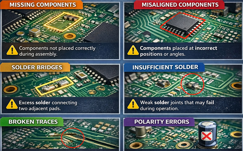
Missing Components
Components not placed correctly during assembly.
Misaligned Components
Components placed at incorrect positions or angles.
Solder Bridges
Excess solder connecting two adjacent pads.
Insufficient Solder
Weak solder joints that may fail during operation.
Broken Traces
Damage to copper traces affecting electrical connections.
Polarity Errors
Components placed with incorrect orientation.
Manual inspection of these defects is extremely difficult due to the small size and complexity of PCB components.
Machine Vision Systems for PCB Inspection
Machine vision systems are widely used in electronics manufacturing to automate PCB inspection. These systems use:
The vision system captures detailed images of the PCB and analyzes them to detect defects automatically.
Types of PCB Inspection Systems
Automated Optical Inspection (AOI)
AOI systems inspect PCBs using cameras and image processing software.
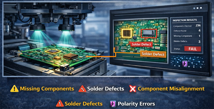
AOI systems are commonly used to detect:
- Missing components
- Solder defects
- Component misalignment
- Polarity errors
3D PCB Inspection
3D inspection systems measure component height and solder joint volume using structured lighting or laser scanning.
This helps detect defects such as:
- Insufficient solder
- Lifted components
- Incorrect solder volume
AI-Based PCB Inspection
AI-powered systems use deep learning algorithms trained on large datasets of PCB images.
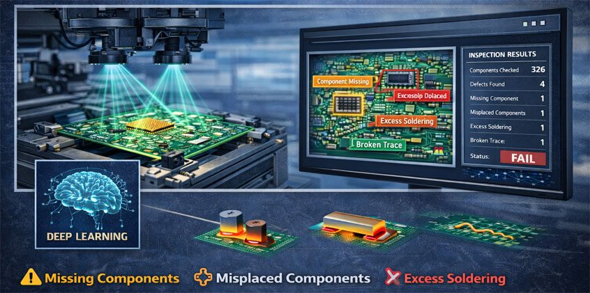
These systems can detect complex defects that traditional rule-based systems may miss.
How AI Improves PCB Inspection
AI and deep learning technologies have significantly improved PCB inspection capabilities. AI-based systems can:
Detect Complex Defects
Identify subtle defects that are difficult to define using rule-based algorithms.
Adapt to PCB Variations
Handle different board designs and component layouts with ease.
Reduce False Positives
Minimize incorrect defect detection through advanced pattern recognition.
Improve Inspection Accuracy
Continuously improve through training with new inspection data.
These capabilities make AI particularly valuable for high-density PCB inspection.
Inspection Workflow
AI-based PCB inspection systems typically follow a structured workflow:
Image Capture
High-resolution cameras capture detailed images of the PCB.
Lighting Control
Specialized lighting highlights components and solder joints.
Image Processing
The system processes images and extracts relevant features.
AI Defect Detection
AI models analyze the PCB image to identify defects.
Pass/Fail Classification
Each PCB is classified as acceptable or defective.
Defect Reporting
The system records inspection data for traceability and analysis.
Benefits of AI-Based PCB Inspection
High Inspection Accuracy
AI models detect even small defects with high precision.
Faster Inspection
Automated systems inspect PCBs at production line speed.
Reduced Labor Costs
Automation reduces reliance on manual inspectors.
100% Inspection Coverage
Every PCB can be inspected automatically.
Improved Manufacturing Yield
Early defect detection helps improve production quality and reduce waste.
Applications in Electronics Manufacturing
PCB inspection systems are used across multiple electronics manufacturing processes:
Surface Mount Technology (SMT)
Inspect component placement and solder joints.
Through-Hole Assembly
Verify insertion of through-hole components.
Solder Paste Inspection
Measure solder paste volume before component placement.
Final PCB Inspection
Verify final assembly quality before shipment.
Integration with Smart Manufacturing
Modern PCB inspection systems can integrate with manufacturing infrastructure such as:
This integration enables real-time quality monitoring and production optimization.
Intelgic's PCB Inspection Solutions
Intelgic develops AI-powered machine vision inspection systems for complex electronic manufacturing environments.
These systems enable electronics manufacturers to detect defects early, improve production yield, and maintain consistent product quality.
The Future of PCB Inspection
PCB designs continue to become smaller and more complex. Future inspection systems will increasingly rely on:
These technologies will enable fully automated PCB quality inspection in next-generation electronics manufacturing.
PCB inspection using AI and machine vision systems enables manufacturers to achieve fast, accurate, and reliable defect detection in electronics manufacturing.
By combining industrial cameras, advanced lighting, AI-based analysis, and automated inspection systems, manufacturers can ensure high-quality PCB production while improving efficiency and reducing costs.
As electronics manufacturing continues to evolve, AI-driven inspection systems will become an essential part of modern PCB production lines.