Detect Solder Defects, Missing Components, and PCB Assembly Errors with AI
Printed Circuit Boards (PCBs) are at the heart of nearly every electronic device:
A single defect can compromise the functionality and reliability of an entire electronic assembly:
As PCB designs become more complex, with smaller components, higher component density, and larger board dimensions, traditional manual inspection becomes increasingly challenging.
Intelgic offers a comprehensive AI-powered PCB inspection solution that automatically scans the board, analyzes high-resolution images, and identifies solder defects, missing components, assembly errors, and visible structural defects.
The solution supports configurable inspection recipes for different PCB dimensions, component layouts, and quality requirements.
For large PCB boards, Intelgic uses a movable machine vision imaging system that travels across the PCB surface, captures multiple overlapping images, and inspects each region using advanced AI algorithms.
Why PCB Manufacturers Need Automated AI Inspection
PCB manufacturing and assembly involve multiple precision processes, including component placement, soldering, wire bonding, and final assembly.
Defects introduced during these processes may not always be visible during functional testing, and some defects can cause failures only after prolonged operation. Common challenges include:
Insufficient solder, excess solder, bridging, and abnormal solder joints.
Resistors, capacitors, ICs, connectors, and other components omitted during assembly.
Components installed in the wrong position or orientation.
Visible cracks, scratches, and physical damage to the PCB.
Missing, misplaced, or visibly damaged wire bonds in applicable electronic assemblies.
Hundreds or thousands of inspection checkpoints on a single board.
Fixed imaging systems may struggle to provide sufficient resolution across the entire board.
Manual inspection can be time-consuming and inconsistent, particularly when operators must examine numerous small solder joints and densely populated components.
Automated AI inspection helps manufacturers detect defects earlier, reduce inspection effort, and maintain consistent quality standards.
How Intelgic’s AI-Powered PCB Inspection System Works
Intelgic combines three technologies to inspect PCB assemblies. The system captures detailed images of the board, identifies components and solder joints, and evaluates them against predefined inspection requirements.
PCB Identification and Inspection Recipe Selection
Different PCB models have different dimensions, component layouts, and inspection requirements. Intelgic allows manufacturers to configure an inspection recipe for each PCB model. A recipe can define:
The appropriate recipe can be selected manually or loaded automatically using:
A single inspection system can support multiple PCB designs.
Automated Scanning of Large PCB Boards
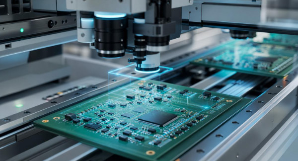
Large PCB boards present a unique imaging challenge. Capturing the entire board in a single image may not provide sufficient detail to detect fine solder defects, microcracks, and small component abnormalities.
Intelgic addresses this challenge with a movable machine vision imaging system that scans the PCB region by region. The imaging system moves across the board in a predefined sequence, capturing multiple high-resolution images from strategic positions.
Illustrative serpentine scan path. Each captured image overlaps its neighbours to reduce gaps in coverage and is tagged with its board coordinates.
The scanning process provides:
The system automatically associates each captured image with its corresponding location on the PCB.
Inspect large and complex PCB assemblies without sacrificing the image detail needed for small defect detection.
AI Defect Detection and Automated Quality Reporting
AI-Based Defect Detection
Once images are captured, Intelgic’s AI analyzes:
The software identifies deviations from expected geometry, component placement, and approved inspection criteria. AI can be configured to recognize both known defect categories and selected visual abnormalities requiring further review.
Each detected defect is classified and linked to its location on the PCB.
Automated PCB Quality Reporting
After completing the inspection, Intelgic generates a comprehensive quality report. The report can include:
The results can be integrated with existing quality management or manufacturing execution systems.
PCB Defects Intelgic’s AI Inspection System Can Detect
Intelgic’s AI inspection solution can be configured to identify a broad range of visible PCB manufacturing and assembly defects.
Solder Joint Defect Detection
Solder defects are among the most critical problems in PCB assembly because they can affect electrical connectivity and long-term product reliability.
Intelgic’s AI analyzes visible solder joints to identify:
These defect categories are consistent with established electronic assembly inspection terminology described in IPC’s soldering troubleshooting guidance.
Helps detect soldering abnormalities before defective boards proceed to final assembly or shipment.
Missing and Incorrect Component Detection
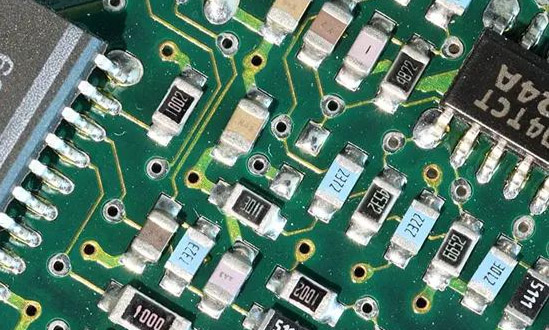
A missing resistor, capacitor, connector, or integrated circuit can cause an electronic assembly to malfunction. Intelgic’s AI compares the actual PCB assembly with the expected component layout. The system can identify:
Where component markings are visible, the system can also compare part identification with the expected assembly configuration.
Reduces component assembly errors and improves PCB manufacturing consistency.
PCB Substrate Crack and Physical Damage Detection
PCB substrates can develop visible damage during manufacturing, handling, soldering, or assembly. Intelgic’s AI can inspect the board surface for:
These defects may affect mechanical integrity, insulation, or electrical reliability.
Helps identify physically damaged boards before they are incorporated into finished products.
Wire Bond, Placement, and Trace Defects
Missing and Damaged Wire Bond Detection
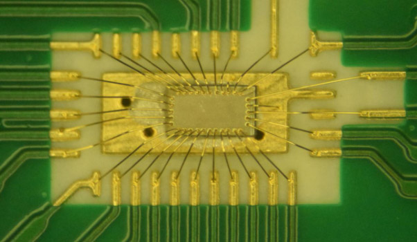
In electronic assemblies containing accessible wire bonds, wire integrity is essential for reliable electrical connections. Intelgic’s AI can be configured to inspect visible wire-bond structures and identify:
The system compares actual wire-bond arrangements with the expected configuration.
Improves inspection of delicate wire-bond assemblies and reduces the risk of undetected visual assembly defects.
Wire bonds enclosed within opaque semiconductor packages cannot be inspected directly using a conventional external imaging system.
Component Orientation and Placement Defects
Components installed incorrectly can cause electrical failures even when solder joints appear acceptable. Intelgic’s AI can detect:
Supports precise component placement verification and helps reduce rework.
PCB Trace and Surface Defects
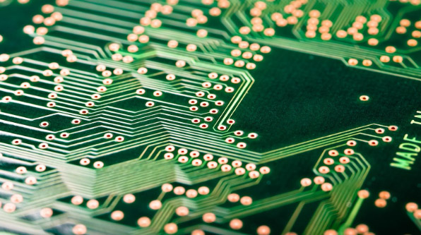
Intelgic’s inspection system can also identify selected visible defects on conductive paths and board surfaces. These include:
For bare-board inspection, the same recipe-based imaging approach can be adapted to compare conductive patterns against approved design references.
Helps identify PCB fabrication and surface-quality problems before downstream assembly.
Complete PCB Defect Inspection at a Glance
Detection performance depends on component visibility, image quality, board geometry, and application-specific AI training and validation.
Configurable Inspection Recipes for Different PCB Sizes and Layouts
One of the important advantages of Intelgic’s system is its recipe-based inspection architecture. Manufacturers frequently produce multiple PCB models with different dimensions, component populations, and inspection requirements.
Instead of creating a separate inspection station for each product, Intelgic allows manufacturers to configure an inspection recipe for every board type. A recipe can store:
When a new PCB model enters production, the system loads the appropriate recipe and automatically adjusts its scanning sequence.
This approach is especially valuable for high-mix PCB manufacturing, where frequent production changeovers are common.
AI-Powered Defect Mapping and Quality Traceability
Intelgic’s inspection software can associate detected defects with specific PCB coordinates and component reference designators.
For example, if the system detects a solder bridge near component U12 or identifies a missing capacitor at C45, the quality report can highlight the corresponding location on the board.
This allows quality engineers to quickly locate defects and take corrective action. The collected data can also support:
Over time, these insights can help manufacturers identify problematic assembly operations and improve production quality.
AI PCB Inspection vs. Traditional Manual Inspection
AI inspection improves consistency and reduces repetitive work, while quality engineers remain important for reviewing uncertain results and validating acceptance criteria.
Applications Across Electronics Manufacturing
ECU boards, control modules, power electronics.
Computer boards, appliances, electronic devices.
PLC boards, controllers, industrial communication modules.
Medical device control boards and electronic assemblies.
High-reliability electronic assemblies.
Communication boards and network equipment.
Power conversion boards and motor controllers.
Accessible wire bonds and package substrate inspection.
Business Benefits of Intelgic’s Automated PCB Inspection
Identify small visible defects across complex PCB assemblies
Automated multi-image scanning across specified inspection regions
Support multiple PCB sizes and component layouts
Automate repetitive inspection and defect localization
Apply standardized inspection criteria across production
Generate part-level defect reports and inspection records
By detecting visible soldering and assembly defects earlier, the system can help reduce rework, prevent defective boards from reaching customers, and improve manufacturing efficiency.
Actual inspection accuracy, throughput, and achievable defect sizes are established during application validation.
Why Choose Intelgic for Automated PCB Inspection?
Intelgic develops AI-powered machine vision solutions for manufacturing quality inspection and process assurance. Our PCB inspection solution combines:
The system can be configured for standalone PCB inspection stations or integrated into automated production workflows.
Intelgic’s objective is to help manufacturers inspect every required PCB region, identify defects earlier, and maintain consistent quality across production.
What Is Required to Automate Your PCB Inspection?
To evaluate an automated inspection application, manufacturers can provide:
PCB dimensions and maximum board size.
Images or sample boards showing acceptable and defective assemblies.
PCB design files, component layout, or BOM where available.
A list of required inspection checkpoints and defect categories.
Minimum defect sizes and acceptance criteria.
Production volume and target inspection cycle time.
Number of different PCB models to be inspected.
Based on these inputs, Intelgic can define a solution tailored to the application:
Inspect the Entire PCB. Detect Defects Before They Become Failures.
PCB quality depends on the reliability of every component, solder joint, and critical board feature. As PCB assemblies become larger and more complex, manufacturers need inspection systems that provide detailed surface coverage and consistent defect detection without relying exclusively on manual inspection.
Intelgic’s AI-powered PCB inspection system combines automated multi-image scanning, intelligent defect detection, and recipe-based inspection to identify solder defects, missing components, visible substrate cracks, wire bond abnormalities, and other manufacturing defects.
From small electronic assemblies to large, densely populated PCB boards, Intelgic provides a flexible approach to automated visual quality assurance.
One intelligent inspection system.
Frequently Asked Questions
What is AI-powered PCB inspection? +
AI-powered PCB inspection uses a machine vision imaging system and AI software to analyze PCB images and detect visible defects such as solder bridges, missing components, incorrect placement, and surface damage.
What solder defects can Intelgic’s AI inspection system detect? +
The system can be configured to identify visible solder bridging, insufficient solder, excess solder, missing solder, solder balls, surface-visible cracks, and abnormal solder joint geometry.
Can Intelgic inspect large PCB boards? +
Yes. For large PCB boards, Intelgic uses a movable machine vision imaging system that scans the board region by region and captures multiple images for AI analysis.
Can the same system inspect different PCB sizes? +
Yes. The system supports configurable inspection recipes defining PCB dimensions, scanning positions, component layouts, and inspection checkpoints.
Can AI detect missing or incorrectly placed PCB components? +
Yes. AI can compare observed component placement with the expected layout and identify missing, misplaced, rotated, or visibly incorrect components.
Can the system detect cracks in PCB substrates? +
Yes. Surface-visible cracks, scratches, chipped edges, and other observable substrate damage can be detected when they fall within the system’s validated imaging capability.
Can Intelgic detect missing wire bonds? +
Yes. For assemblies with accessible wire bonds, the AI can identify missing, visibly broken, or incorrectly positioned wires. Hidden internal bonds require other inspection methods.
Can AI inspect solder joints underneath BGA components? +
Not directly using conventional optical imaging. Hidden BGA solder joints generally require X-ray inspection or another suitable complementary method.
Does the system generate PCB inspection reports? +
Yes. The system can generate reports containing PCB identifiers, defect classifications, locations, images, and inspection pass/fail status.
Can AI inspect every component on a PCB? +
The system can be configured to inspect all specified components and visible checkpoints within the validated scanning coverage. Visibility, component geometry, and achievable resolution determine which defects can be reliably identified.
Can the system identify incorrect component values? +
It may identify an incorrect component when visible markings or physical differences distinguish it from the expected part. Electrical verification is required when values cannot be reliably determined visually.
Can Intelgic’s system integrate with existing PCB production lines? +
Yes. The system can integrate with production equipment and manufacturing software for inspection triggering, recipe selection, result reporting, and quality traceability.
Is AI PCB inspection suitable for high-mix, low-volume manufacturing? +
Yes. Recipe-based inspection can support different PCB models and changing production requirements, although each recipe must be configured and validated.
How does Intelgic improve inspection coverage on large PCBs? +
The imaging system moves across the PCB and captures multiple overlapping images at predefined locations, providing detailed coverage of the required inspection regions.
How can manufacturers get started with Intelgic’s PCB inspection solution? +
Manufacturers can share PCB drawings, board dimensions, component layouts, defect samples, and inspection requirements. Intelgic can then evaluate the scanning configuration and AI inspection approach.