Micron-Level Surface Defect Detection in PCBs Using Machine Vision AOI
Published on: May 02, 2025

Written by: Content team, Intelgic
Micron-Level Surface Defect Detection in PCBs Using Machine Vision AOI
In the fast-paced world of electronics manufacturing, Printed Circuit Boards (PCBs) are the heart of virtually every modern device. As demand grows for smaller, more complex, and highly reliable electronics, the margin for error in PCB production continues to shrink. Even the tiniest surface defect—measured in microns—can result in product failure, leading to significant financial and reputational losses for manufacturers.
To address this, cutting-edge Machine Vision Automated Optical Inspection (AOI) systems have emerged as an essential solution. By combining high-resolution imaging, intelligent illumination systems, and AI-driven analytics, manufacturers can now detect and classify PCB surface defects with unmatched precision and speed.
Types of Surface Defects in PCBs
Surface defects on PCBs can originate from various stages of the manufacturing process—ranging from material handling to etching, plating, and soldering. Identifying and addressing these defects at the micron level is essential to ensuring electrical performance, product safety, and longevity.
Below are some of the most commonly encountered and critical surface-level defects:
- Solder Bridges
Unintentional connections between adjacent solder pads or component leads, creating potential short circuits.
- Pinholes and Voids
Tiny holes or gaps within solder joints or plated areas that weaken the mechanical and electrical integrity of the board.
- Hairline Cracks / Micro-cracks
Very fine, nearly invisible fractures in copper traces or solder joints, often caused by thermal stress or mechanical shock.
- Foreign Particles and Contamination
Presence of dust, fibers, flux residues, or chemical deposits that may lead to corrosion, conductivity issues, or shorting.
- Component Misalignment
Incorrect orientation or positioning of surface-mounted components, which may result in failed connections or poor signal performance.
- Insufficient / Excess Solder
Inadequate solder can result in cold joints or open circuits, while excess solder can cause bridging and reliability issues.
- Scratches and Abrasions
Physical surface damage caused by improper handling or defective equipment, which can sever conductive paths or expose inner layers.
- Spur
A thin, unintended metallic protrusion from a trace or pad, often a result of over-etching or plating anomalies. Spurs can detach and cause shorts.
- Spurious Copper (Copper Slivers)
Unintended small fragments or slivers of copper on the PCB surface due to improper etching. These can move or flake off, creating unpredictable failures.
- Missing Holes
A critical defect where a plated through-hole (PTH) or via is either not drilled or improperly formed, leading to open circuits or broken interconnections.

Challenges in Detecting Micron-Level PCB Defects
Inspection at the micron level introduces several technical and operational challenges, particularly when working with compact PCBs like the 100-115 mm variants used in high-density electronics. Key challenges include:
- Small Component Spacing and Fine Details
With a high concentration of pads, traces, and components in a limited space, it becomes difficult to distinguish between acceptable variations and actual defects without high-resolution optics.
- High-Density Layouts
The densely packed architecture increases the likelihood of defects such as solder bridging, spurious copper, and missing holes—especially when spacing between features is minimal.
- Complex Surface Topography
The combination of flat regions, raised solder joints, vias, and irregular textures creates a varied surface that challenges traditional inspection systems.
- Material Reflectivity and Surface Finish
PCBs incorporate multiple surface materials—like copper, solder mask, and flux residues—that reflect light differently. This makes defects such as micro-cracks, scratches, or spurs difficult to spot under standard lighting.
- Speed and Production Throughput
High-speed production lines leave no room for slow or manual inspection processes. The AOI system must perform inspections in real time, maintaining high accuracy without slowing down the assembly line.
- Similar Appearance of Defects and Design Elements
Defects like mouse bites, spurious copper, missing holes, and burrs can closely resemble legitimate design features. Distinguishing between them requires intelligent pattern recognition and defect classification.
- Frequent Design Changes and Product Variants
In industries with rapid development cycles, inspection systems must be flexible enough to accommodate new PCB layouts, materials, and component profiles with minimal reprogramming.
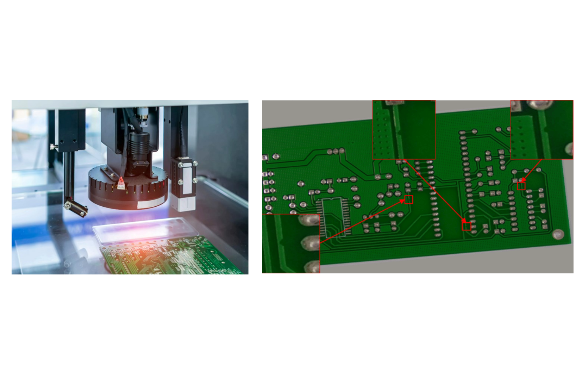
How Area Scan Cameras and Advanced Illumination Tackle These Challenges
Area scan cameras play a crucial role in the precise inspection of printed circuit boards (PCBs) by capturing high-resolution, full-frame 2D images. Unlike line scan cameras, which require precise synchronization with mechanical motion to build a complete image line-by-line, area scan cameras provide a complete field-of-view in a single exposure. This capability makes them particularly suitable for applications where the object is stationary or when capturing an entire area at once is advantageous.
These cameras are equipped with advanced high-resolution sensors, enabling them to detect minute variations and anomalies across the PCB surface. Their key advantages include:
- Wide Field-of-View: Ideal for inspecting multiple components or entire sections of the PCB in a single shot, improving throughput and reducing system complexity.
- High-Speed Image Acquisition: Facilitates real-time inspection and analysis, essential for modern automated manufacturing lines.
- Detection of Irregular and Small Defects: Capable of identifying subtle imperfections, such as micro-cracks, misalignments, or residue, which may compromise PCB performance.
To maximize the effectiveness of area scan cameras, sophisticated illumination techniques are employed to mitigate challenges posed by reflective surfaces, variable textures, and fine structural details. These lighting strategies include multi-angle and multi-spectral systems that highlight features otherwise invisible under standard lighting conditions.
Some examples of advanced illumination methods include:
- Dark-Field Illumination: Projects light at shallow angles, making surface scratches, dents, and other topographical defects visible through contrast-enhancing shadows.
- Coaxial Illumination: Uses beam-splitters to direct light directly onto the surface, enhancing the visibility of flat surface details, such as color variations, silkscreen inconsistencies, and subtle texture differences.
- Structured Light: Projects patterned light to generate depth information, useful for analyzing layered or uneven surfaces.
AI Software: The Intelligence Behind Speed and Precision
While imaging hardware captures what’s on the surface, the true intelligence lies in AI-driven software that interprets the data.
Intelgic’s Live Vision AI Software leverages machine learning and deep learning models trained on vast datasets of PCB images. These models are capable of:
- Identifying patterns and anomalies that deviate from acceptable standards
- Learning from new defect types over time to improve accuracy
- Minimizing false positives that typically slow down production or require unnecessary manual verification
Prioritizing defects based on severity, ensuring only critical issues halt production
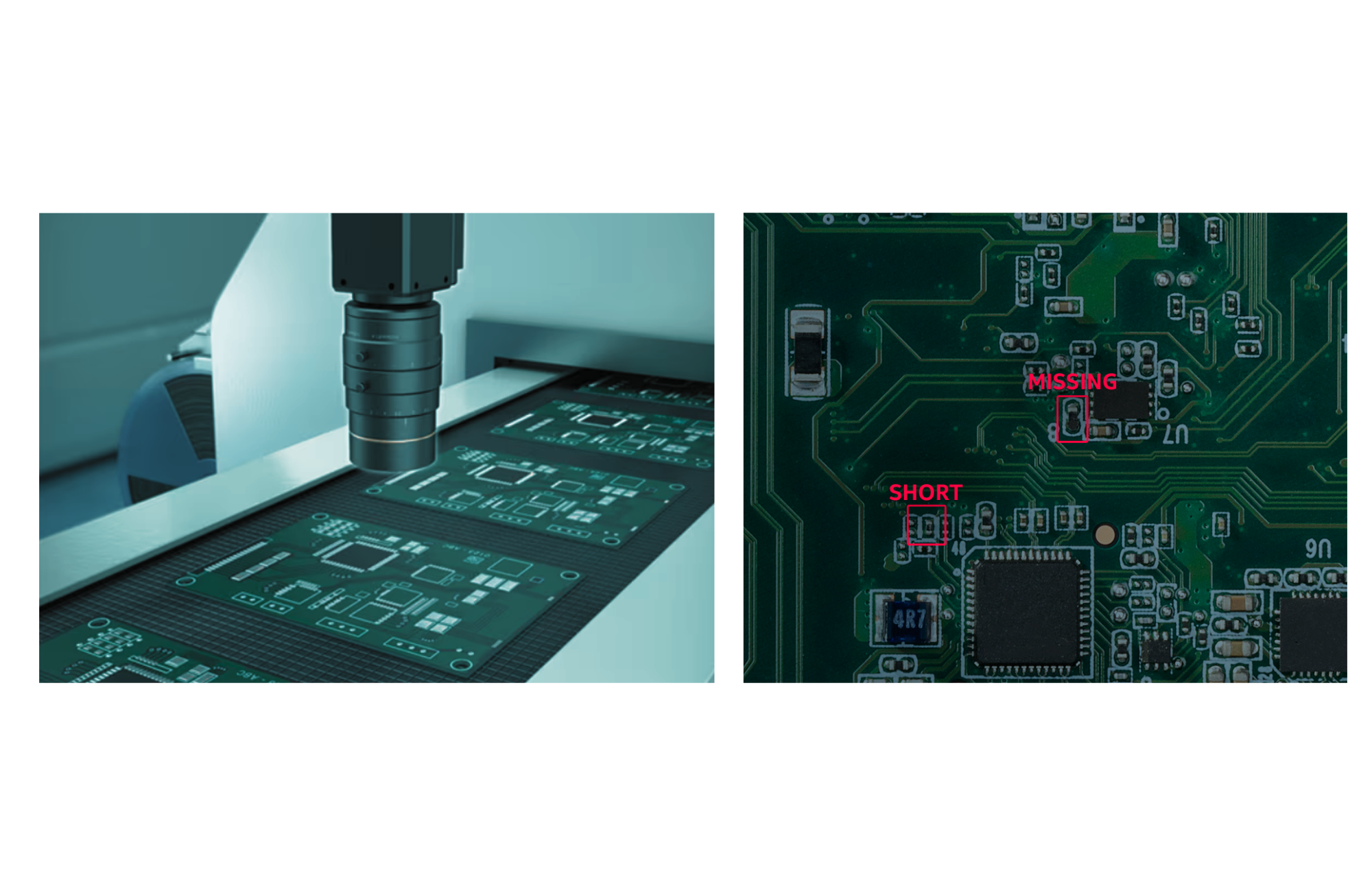
Machine Vision AOI Process for PCB Inspection: A Step-by-Step Overview
- PCB Loading: The PCB enters the inspection station through a conveyor or robotic handler.
- High-Resolution Imaging: Area scan cameras capture images using optimized illumination configurations.
- Image Preprocessing: The system corrects lighting variations, normalizes the background, and enhances image clarity.
- Defect Detection & Classification: AI algorithms analyze the image for defects and categorize them based on type and severity.
- Data Reporting: Results are presented in a user-friendly interface, highlighting defect locations, images, and suggested actions.
- Integration with MES/ERP: Data is logged and fed into the manufacturing ecosystem for traceability, analytics, and quality improvement.
- Feedback Loop: Continuous learning enables the system to improve with each inspection.
Emerging Trends in Automated Optical Inspection (AOI)
The field of Automated Optical Inspection (AOI) is advancing at a rapid pace, driven by innovations in artificial intelligence, sensor technology, and data analytics. These developments are shaping the future of electronics manufacturing by enhancing inspection accuracy, speed, and adaptability. In the coming years, manufacturers can expect the following transformative trends to become integral to AOI systems:
- 3D AOI Integration: The convergence of 2D and 3D inspection technologies enables a more comprehensive analysis of PCB assemblies. While 2D imaging captures surface-level details, 3D AOI adds depth information, allowing for the detection of volumetric defects such as solder joint height variations, lifted leads, and component tilt—critical factors in ensuring structural and electrical integrity.
- Edge AI Deployment: By embedding AI algorithms directly within AOI hardware, edge AI allows for real-time decision-making without relying on external computing resources. This localized processing significantly reduces latency, enhances inspection speed, and enables smarter defect classification at the point of data capture.
- Cloud-Based Learning and Model Sharing: Centralized training of AI models using aggregated data from multiple production lines and facilities allows for continuous improvement in defect recognition. These cloud-connected systems can update AOI algorithms across all deployed units, ensuring consistency and leveraging collective learning from a global knowledge base.
- Self-Optimizing Inspection Systems: Future AOI systems will incorporate AI-driven self-adjustment capabilities, dynamically tuning lighting conditions, camera settings, and inspection parameters based on the specific PCB design, material reflectivity, and defect history. This level of automation minimizes human intervention and maximizes inspection reliability.
- Predictive Quality Control: Leveraging historical inspection data and trend analysis, predictive models will forecast potential defect occurrences before they happen. This proactive approach enables early intervention, process adjustments, and reduced scrap rates—contributing to higher overall yield and manufacturing efficiency.
Why Intelgic’s Smart AOI Solution Stands Out
Intelgic offers a next-generation AOI solution that integrates high-performance machine vision with smart AI algorithms tailored for PCB inspection. Key differentiators include:
- Micron-level detection capability with ultra-high-resolution area scan cameras
- Adaptive AI algorithms trained for dynamic learning across various PCB types
- Modular, configurable lighting systems that adjust to the PCB’s reflectivity and layout
- Real-time defect feedback and MES integration for proactive quality control
- Live Vision software with a rich interface for visualization, manual override, and audit logging
Micron-level defect detection is no longer an option but a necessity in modern PCB production. The integration of machine vision, high-precision imaging, advanced illumination, and AI analytics empowers manufacturers to ensure quality at scale without compromising speed or cost.
Intelgic’s smart AOI solution exemplifies this technological synergy—bringing together innovation, intelligence, and industrial-grade reliability. For manufacturers aiming to maintain a competitive edge and meet the ever-growing demand for precision electronics, embracing machine vision AOI is a strategic step toward the future of intelligent, defect-free production.